Andhra Pradesh BIEAP AP Inter 2nd Year Physics Study Material 15th Lesson Semiconductor Electronics: Material, Devices and Simple Circuits Textbook Questions and Answers.
AP Inter 2nd Year Physics Study Material 15th Lesson Semiconductor Electronics: Material, Devices and Simple Circuits
Very Short Answer Questions
Question 1.
What is an n-type semiconductor? What are the majority and minority charge carriers in it?
Answer:
If a pentavalent impurity is added to a pure tetravalent semiconductor, it is called an n-type semiconductor.
In n-type semiconductor majority, of charge carriers are electrons and the minority charge carriers are holes.
Question 2.
What are intrinsic and extrinsic semiconductors? (A.P. Mar. ’15)
Answer:
Pure form of semiconductors are called intrinsic semiconductors.
When impure atoms are added to increase their conductivity, they are called extrinsic semiconductors.
![]()
Question 3.
What is a p-type semiconductor ? What are the majority and minority charge carriers in it?
Answer:
If a trivalent impurity is added to a tetravalent semiconductor, it is called p-type semi-conductor.
In p-type semiconductor majority charge carriers are holes and minority charge carriers are electrons.
Question 4.
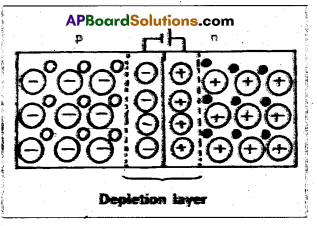
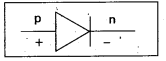
What is a p-n junction diode ? Define depletion layer. (T.S. Mar. ’19)
Answer:
When an intrinsic semiconductor crystal is grown with one side doped with trivalent element and on the other side doped with pentavalent element, a junction is formed in the crystal. It is called p-n junction diode.
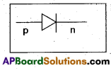
A thin narrow region is formed on either side of the p-n junction, which is free from charge carriers is called depletion layer.
Question 5.
How is a battery connected to a junction diode in
- forward and
- reverse bias ?
Answer:
- In p-n junction diode, if p-side is connected to positive terminal of a cell and n-side to negative terminal, it is called forward bias.
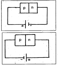
- In a p-n junction diode, p-side is connected to negative terminal of a cell and n-side to positive terminal, it is called reverse bias.
![]()
Question 6.
What is the maximum percentage of rectification in half wave and full wave rectifiers ?
Answer:
- The percentage of rectification in half-wave rectifier is 40.6%.
- The percentage of rectification in full-wave rectifier is 81.2%.
Question 7.
What is Zener voltage (Vz) and how will a Zener diode be connected in circuits generally ?
Answer:
- When Zener diode is in reverse biased, at a particular voltage current increases suddenly is called Zener (or) break down voltage.
- Zener diode always connected in reverse bias.
Question 8.
Write the expressions for the efficiency of a full wave rectifier and a half wave rectifier.
Answer:
- Efficiency of half wave rectifier (η) = \(\frac{0.406 \mathrm{R}_{\mathrm{L}}}{\mathrm{r}_{\mathrm{f}}+\mathrm{R}_{\mathrm{L}}}\)
- Efficiency of full wave rectifier (η) = \(\frac{0.812 \mathrm{R}_{\mathrm{L}}}{\mathrm{r}_{\mathrm{f}}+\mathrm{R}_{\mathrm{L}}}\)
Question 9.
What happens to the width of the depletion layer in a p-n junction diode when it is
i) forward-biased and
ii) reverse biased ?
Answer:
When a p-n junction diode is forward bias, thickness of depletion layer decreases and in reverse bias, thickness of depletion layer increases.
Question 10.
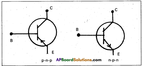
Draw the circuit symbols for p-n-p and n-p-n transistors. (Mar. 14) (A.P. Mar. 19; T.S. Mar. 16)
Answer:
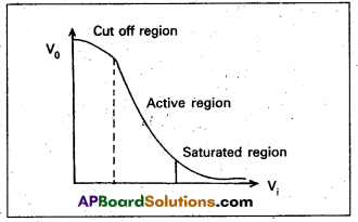
Question 11.
Deflne amplifier and amplification factor.
Answer:
- Rising the strength of a weak signal is known as amplification and the device is called amplifier.
- Amplification factor is the ratio between output voltage to the input voltage.
A = \(\frac{\mathrm{V}_0}{\mathrm{~V}_{\mathrm{i}}}\)
![]()
Question 12.
In which bias can a Zener diode be used as voltage regulator ?
Answer:
In reverse bias Zener diode can be used as voltage regulator.
Question 13.
Which gates ae called universal gates ?
Answer:
NAND gate and NOR gates are called universal gates.
Question 14.
Write the truth table of NAND gate. How does it differ from AND gate.
Answer:
Short Answer Questions
Question 1.
What are n-type and p-type semiconductors? How is a semiconductor junction formed?
Answer:
n-type semiconductor : When a pure semiconductor is droped with pentavalent atoms like Arsenic, Antimony, Bismuth, then n-type semiconductor is formed.
p-type semiconductor: When a pure semiconductor is doped with trivalent atoms like Indium, Gallium. Al, p-type semiconductor is formed.
Formation of p-n junction diode: When p-type and n-type semiconductors are formed side by side at the junction, holes from p side diffuse to the n -side and electrons from n -side to p-side.
Hence positive charge is built in n-side and negative charge is established at the p-side.
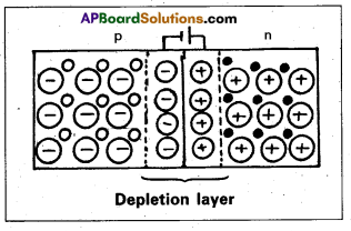
At the junction, the electrons and holes recombine and the region is free from charge carriers. This region which is free from charge carriers is called depletion layer.
The potential developed near the p-n junction is called barrier potential.
The potential barrier stops further diffusion of holes and electrons across the junction.
![]()
Question 2.
Discuss the behaviour of p-n junction. How does a potential barrier develop at the junction ?
Answer:
When p-n junction is formed, the free electrons on n-side diffuse over to p-side, they combine with holes and become neutral. Similarly holes on p-side diffuse over to n-side and combine with electrons become neutral.
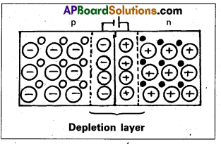
This results in a narrow region formed on either side of the junction. This region is called depletion layer. Depletion layer is free from charge carriers.
The n-type material near the junction becomes positively charged due to immobile donor ions and p-type material becomes negatively charged due to immobile acceptor ions. This creates an electric field near the junction directed from n-region to p-region and causes a potential barrier.
The potential barrier stops further diffusion of holes and electrons across the junction. The value of the potential barrier depends upon the nature of the crystal, its temperature and the amount of doping.
Question 3.
Draw and explain the current-voltage (I -V) characteristic curves of a junction diode in forward and reverse bias.
Answer:
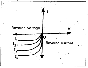
A graph is drawn between the applied voltage (V) and the current (I) passing through the p-n junction diode is called characteristics of a diode.
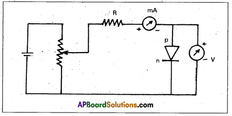
As forward bias voltage is increased potential barrier decreases, but initially increases in current is negligible (region OA). This is due to the potential barrier.
The voltage at which the current starts to increase rapidly is called knee voltage (or) cut in voltage.
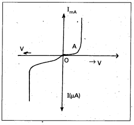
In this reverse bias, small current flows in the circuit due to minority charge carriers. 1f the reverse voltage is increased further, after some voltage, there will be a sudden rise of reverse current. This region is named as breakdown region.
![]()
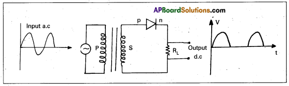
Question 4.
Describe how a semiconductor diode is used as a half wave rectifier. (Mar. ’14) (T.S. & A.P. Mar. ’16)
Answer:
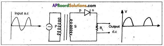
- A half wave rectifier can be constructed with a single diode. The ac input signal is fed to the primary coil of a transformer. The output .signal is taken across the load resistance RL
- During positive half cycle, the diode is forward biased and current flows through the diode.
- During negative half cycle, diode is reverse biased and no current flows through the load resistance.
- This means current flows through the diode only during positive half cycles and negative half cycles are blocked. Hence in the output we get only positive half cycles.
- Rectifier efficiency is defined as the ratio of output dc power to the input ac power.
η = \(\frac{\mathrm{P}_{\mathrm{dc}}}{\mathrm{P}_{\mathrm{ac}}}\) = \(\frac{0.406 \mathrm{R}_{\mathrm{L}}}{\mathrm{r}_{\mathrm{f}}+\mathrm{R}_{\mathrm{L}}}\)
where rf = Forward resistance of a diode; RL = Load resistance
The maximum efficiency of half wave rectifier is 40.6%.
Question 5.
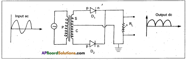
What is rectification ? Explain the working of a full wave rectifier. (T. S. Mar. 19: A.P. & T.S. Mar. ’15)
Answer:
Rectification : The process of converting on alternating current into a direct current is called rectification.
The device used for this purpose is called rectifier.
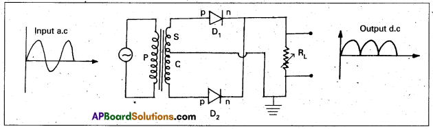
- A full wave rectifier can be constructed with the help of two diodes D1 and D2.
- The secondary transformer is centre tapped at C and its ends are connected to the p regions of two diodes D1 & D2.
- The output voltage is measured across the load resistance RL.
- During positive half cycles of ac, the diode D1 is forward biased and current flows through the load resistance RL. At this time D2 will be reverse biased and will be in switch off position.
- During negative half cycles of ac, the diode D2 is forward biased and the current flows through RL. At this time D1 will be reverse biased and will be in switch off position.
- Hence positive output is obtained for all the input ac signals.
- The efficiency of a rectifier is defined as the ratio between the output dc power to the input ac power.
η = \(\frac{\mathrm{P}_{\mathrm{dc}}}{\mathrm{P}_{\mathrm{ac}}}\) = \(\frac{0.812 \mathrm{R}_{\mathrm{L}}}{\mathrm{r}_{\mathrm{f}}+\mathrm{R}_{\mathrm{L}}}\)
The maximum efficiency of a full wave rectifier is 81.2%
Question 6.
Distinguish between half-wave and full-wave rectifiers. (A.P. Mar. ’19)
Answer:
Half wave rectifier
- Single diode is used.
- Only half wave is rectified.
- Rectifier efficiency η = \(\frac{0.406 \mathrm{R}_{\mathrm{L}}}{\mathrm{r}_{\mathrm{f}}+\mathrm{R}_{\mathrm{L}}}\)
- Efficiency of half wave rectifier is 40.6%.
- Output is discontinuous and pulsative.
Full wave rectifier
- Two diodes are used.
- Full wave is rectified.
- Rectifier efficiency η = \(\frac{0.812 \mathrm{R}_{\mathrm{L}}}{\mathrm{r}_{\mathrm{f}}+\mathrm{R}_{\mathrm{L}}}\)
- Efficiency of full wave rectifier is 81.2%.
- Output is continuous and pulsative.
![]()
Question 7.
Distinguish between zener breakdown and avalanche breakdown.
Answer:
Zèner break down
- Zener break down occurs at heavily doped diodes.
- This occurs at low reverse bias voltages.
- This occurs due to field emissîon.
- Width of depletion layer is small.
Avalanche break down
- Avalanche break down occurs at lightly doped diodes.
- This occurs at high reverse bias voltages.
- This occurs due to ionisation by collision.
- Width of depletion layer is also small.
Question 8.
Explain hole conduction in intrinsic semiconductors.
Answer:
Pure semiconductors are called intrinsic semiconductors. At low temperature, valency band is filled with electrons and conduction band is empty. Hence it acts as an insulator at low temperature.
As temperature increases electrons in valence band get energy and jumps into the conduction band crossing the forbidden band. At their places in the valency band a vacancy is created.
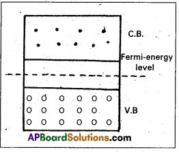
This vacancy of electron in the valency band is called a hole. Hole has positive charge and move only in the valency band; giving hole current.
In this Fermi-energy level will be at the middle of the forbidden band.
Question 9.
What is a photodiode ? Explain its working with a circuit diagram and draw its I-V characteristics.
Answer:
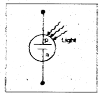
Photodiode : Photodiode is an optoelectronic device in which current carriers are generated by photons through photo excitation.
Working : When visible light of energy greater than forbidden energy gap is incident on a reverse biased p-n juncton photodiode, additional electron-hole pairs are created in the depletion layer (near the junction). These charge carriers will be seperated by the junction field and made to flow across the junction. Creating a reverse current across the junction.
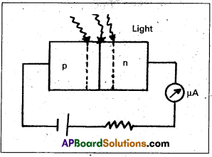
The value of reverse saturation current increases with the increase in the intensity of incident light.
V-I characteristics of photodiode is shown in figure. It is found that reverse saturation current through the photodiode varies almost linearly with the light flux.
Uses :
- It is used in switching the light ON and OFF.
- It is used in demodulation in optical signals.
![]()
Question 10.
Explain the working of LED and what are its advantages over conventional incandescent low power lamps.
Answer:
Light emitting diode (LED) : It is a photoelectronic device which converts electrical energy into light energy.
It is a heavily doped p-n junction diode which under forward bias emits spontaneous radiation. The diode is covered with a transparent cover so that the emitted light may be come out.
Working ; When p-n junction diode is forward biased, the movement of majority charge carriers takes place across the junction. The electrons move from n-side to p-side through the junction and holes move from p-side to n-side.
As a result of it, concentration of majority carriers increases rapidly at the junction.
When there is no bias across the junction, therefore there are excess minority carriers on either side of the junction, which recombine wito majority carriers near the junction.
On recombination of electrons and hole, die energy is given out in the form of heat and light.
Advantages of LED’S over incandescent lamp:
- LED is cheap and easy to handle.
- LED has less power and low operational voltage.
- LED has fast action and requires no warm up time.
- LED can be used in burglar alarm system.
Question 11.
Explain the working of a solar cell and draw Its I-V characteristics.
Answer:
Solar cell is a p-n junction device which converts solar energy into electric energy.
It consists of a silicon (or) gallium – arsenic p-n junction diode packed in a can with glass window on top. The upper layer is of p-type semiconductor. It is very thin so that the incident light photons may easily reach the p-n junction.
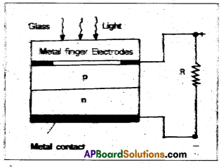
Working : When light (E = hv) falls at the junction, electron – hole pairs are generated near 13% junction. The electrons and holes produced move in opposite directions due to junction field. They will be collected at the two sides of the junction giving rise to a photo voltage between top and bottom metal electrodes. Top metal acts as positive electrode and bottom metal acts as a negative electrode. When an external load is connected across metal electrodes a photo current flows.
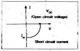
I – V characteristics : I – V characteristics of solar cell is drawn in the fourth quadrant of the co-ordinate axes. Because it does not draw current.
Uses : They are used in calculators, wrist watches, artificial satellites etc.
![]()
Question 12.
Explain the different transistor configurations with diagrams.
Answer:
There are three configurations. They are
1) Common Base
2) Common emitter
3) Common collector.
1) Common Base configuration :
In this configuration base is earthed. Base is common both input and output. Input is given across base – emitter and output is taken across base-collector.
2) Common Emitter configuration :
In this configuration emitter is earthed. Emitter is common both input and output. Input is given across base – emitter and output is taken across collector – emitter.
3) Common collector configuration :
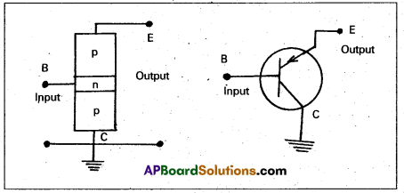
In this configuration collector is earthed. Collector is common both input and output. Input is given across base collector and output is taken across collector – emitter.
Question 13.
Explain how transistor can be used as a switch?
Answer:
To understand the operation of transistor as a switch.
- As long as Vi is low and unable to forward bias the transistor, V0 is high (at VCC).
- If Vi is high enough to drive the transistor into saturation then V0 is low, very near to zero.
- When the transistor is not conducting it is said to be switched off and when it is driven into saturation it is said to be switched on.
- We can say that a low input to the transistor gives a high output and high input gives a low output.
- When the transistor is used in the cutoff (or) saturation state it acts as a switch.
Question 14.
Explain how transistor can be used as an oscillator ?
Answer:
- In an oscillator, we get ac output without any external input signal.
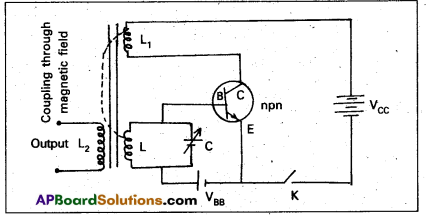
- Here L – C circuit is inserted in emitter-base circuit of transistor winch is forward biased with battery VBB. The collector emitter circuit is reverse biased with battery VCC-.
- A coil L1 is inserted in collector emitter circuit. It is coupled with L.
Working:
- S we close the key (K), weak collector current start rising with time due to inductance L1. As a resell, increasing magnetic flux is finked with L1 and L.
- Due to mutual induction, an emf is induced in L which will charge the upper plate of capacitor (C), consequently there will be support to the forward biasing of emitter base circuit.
- This results in an increasing in the emitter current and hence an increase in the collector current.
- Due to it, more increasing magnetic flux is linked with L1 & L.
- The above process continues till the collector current becomes maximum (or) saturated,
- The resonant frequency of tuned circuit at which the oscillator will oscillate.
v = \(\frac{1}{2 \pi \sqrt{L C}}\)
![]()
Question 15.
Define WND and NOR gases. Give their truth tables.
Answer:
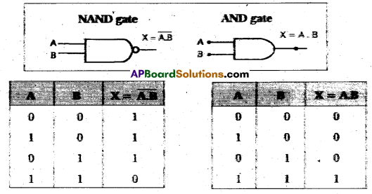
NAND gate : NAND gate is a combination of AND gate and NOT gate.
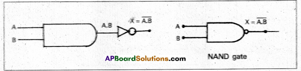
NAND gate can be obtained by connecting a NOT gate in the output of an AND gate. NAND gates are called universal gates.
- If both inputs are low, output is high
A = 0, B = 0, X = 1
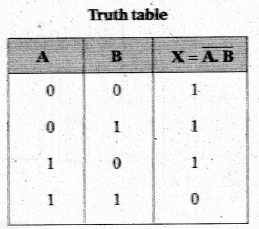
- If any input is low, output is high.
A = 0, B = 1, X = 1
A = 1, B = 0, X = 1 - If both inputs are high, output is low.
A = 1, B = 1, X = 0
NOR gate : NOR gate is a combination of OR gate and NOT gate when the output of OR gate is connected to NOT gate. It has two (or) more inputs and one output.
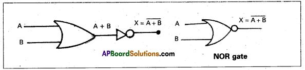
- If both inputs are low, output is high
A = 0, B = 0, X = 1
- If input is high, output is low.
A = 0, B = 0, X = 1 - If both inputs are high, the output is low.
A = 1, B = 1, X = 0
NOR gate is also a universal gate.
![]()
Question 16.
Explain the operation of a NOT gate and give, its truth table.
Answer:
NOT gate: NOT gate is the basic gate. It has one input and one output. The NOT gate is also called an inverter. The circuit symbol of NOT gate is shown in figure.
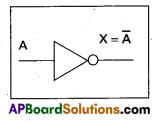
- If input is low, output is high.
A = 0, X = \(\overline{0}\) = 1
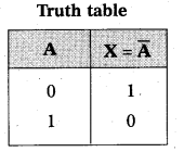
- If input is high, output is low.
A = 1, X = \(\overline{1}\) = 0
Long Answer Questions
Question 1.
What is a junction diode ? Explain the formation of depletion region at the junction. Explain the variation of depletion region in forward and reverse-biased condition.
Answer:
p-n junction diode: When a p-type semiconductor is suitably joined to n-type semiconductor, a p-n junction diode is formed.
The circuit symbol of p-n junction diode is shown in figure.
Formation of depletion layer at the junction: When p-n junction is formed, the free electrons on n-side diffuse over to p-side, they combine with holes and become neutral. Similarly holes on p-side diffuse over to n-side and combine with electrons become neutral.
This results in a narrow region formed on either side of the junction. This region is called depletion layer. Depletion layer is free from charge carriers.
The n-type material near the junction becomes positively charged due to immobile donor ions and p-type material becomes negatively charged due to immobile acceptor ions. This creates an electric field near the junction directed from n-region to p-region and cause a potential barrier.
The potential barrier stops further diffusion of holes and electrons across the junction. The value of the potential barrier depends upon the nature of the crystal, its temperature and the amount of doping.
Forward bias:
“When a positive terminal of a battery is connected to p-side and negative terminal is connected to n-side; then p-n junction diode is said to be forward bias”.
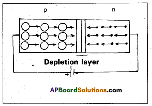
The holes in the p-region are repelled by the positive polarity and move towards the junction.
Similarly electrons in the n-region are repelled by the negative polarity and move towards the junction.
As a result, the width of the depletion layer decreases. The charge carriers cross the junction and electric current flows in the circuit.
Hence in forward bias resistance of diode is low. This position is called switch on position.
Reverse bias:
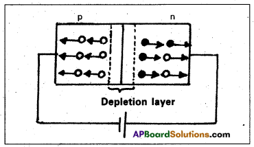
‘When the negative terminal of the battery is connected to p-side and positive terminal of the battery is connected n-side of the p-n junction, then the diode is said to be reverse bias”.
The holes in the p-region are attracted towards negative polarity and move away from the junction. Similarly the electrons in the n-region are attracted towards positive polarity and move away from the junction.
So, width of the depletion layer and potential barrier increases. Hence resistance of p-n junction diode increases. Thus the reverse biased diode is called switch off position.
Question 2.
What is a rectifier ? Explain the working of half wave and full wave rectifiers with diagrams.
Answer:
Rectifier: It is a circuit which converts ac into d.c. A p-n junction diode is used as a rectifier.
Half-wave rectifier:
- A half wave rectifier can be constructed with a single diode. The ac input signal is fed to the primary coil of a transformer. The output signal is taken across the load resistance RL.
- During positive half cycle, the diode is forward biased and current flows through the diode.
- During negative half cycle, diode is reverse biased and no current flows through the load resistance.
- This means current flows through the diode only during positive half cycles and negative half cycles are blocked. Hence in the output we get only positive half cycles.
- Rectifier efficiency is defined as the ratio of output dc power to the input ac power.
η = \(\frac{\mathrm{P}_{\mathrm{dc}}}{\mathrm{P}_{\mathrm{ac}}}\) = \(\frac{0.406 \mathrm{R}_{\mathrm{L}}}{\mathrm{r}_{\mathrm{f}}+\mathrm{R}_{\mathrm{L}}}\)
Where rf = Forward resistance of a diode; RL = Load resistance
The maximum efficiency of half wave rectifier is 40.6%.
Full wave rectifier: The process of converting an alternating current into a direct current is called rectification.
The device used for this purpose is called rectifier.
- A full wave rectifier can be constructed with the help of two diodes D1 and D2.
- The secondary transformer is centre tapped at C and its ends are connected to the p regions of two diodes D1 & D2.
- The output voltage is measured across the load resistance RL.
- During positive half cycles of ac, the diode D1 is forward biased and current flows through the load resistance RL. At this time D2 will be reverse biased and will be in switch off position.
- During negative half cycles of ac, the diode D2 is forward biased and the current flows through RL. At this time D1 will be reverse biased and will be in switch off position.
- Hence positive output is obtained for all the input ac signals.
- The efficiency of a rectifier is defined as the ratio between the output dc power to the input ac power.
η = \(\frac{\mathrm{P}_{\mathrm{dc}}}{\mathrm{P}_{\mathrm{ac}}}\) = \(\frac{0.812 \mathrm{R}_{\mathrm{L}}}{\mathrm{r}_{\mathrm{f}}+\mathrm{R}_{\mathrm{L}}}\)
The maximum efficiency of a full wave rectifier is 81.2%.
![]()
Question 3.
What is a Zener diode ? Explain how it is used as a voltage regulator.
Answer:
Zener diode : Zener diode is a heavily doped germanium (or) silicon p-n junction diode. It works on reverse bias break down region.
The circuit symbol of zener diode is shown in figure.
Zener diode can be used as a voltage regulator. In general zener diode is connected in reverse bias in the circuits.
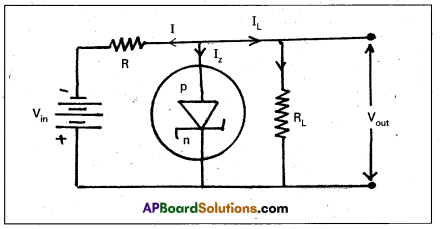
- The zener diode is connected to a battery, through a resistance R. The battery reverse biases the zener diode.
- The load resistance RL is connected across the terminals of the zener diode.
- The value of R is selected in such away that in the absence of load RL maximum safe current flows in the diode.
- Now consider that load is connected across the diode. The load draws a current.
- The current through the diode falls by the same amount but the voltage drops across the load remains constant.
- The series resistance R absorbs the output voltage fluctuations, so as to maintain constant voltage across the load.
- The voltage across the zener diode remains constant even if the load RL varies. Thus, zener diode works as voltage regulator.
- If I is the input current, IZ and IL are zener and load currents.
I = IZ + IL; Vin = IR + VZ
But Vout= VZ
∴ Vout= Vin – IR
Question 4.
Describe a transistor and explain its wbking.
Answer:
Transistor: It is a device which consists of two p-n junctions joined back to back. Transistor means transfer of resistance.
Transistor has three regions. They are :
1) Emitter (E)
2) Base (B)
3) Collector (C)
1) Emitter (E) The section at one end of transistor is called emitter. It is heavily doped region. It emitts charge carriers.
2) Base (B) : The middle section off transistor is called base. This is lightly doped and very thin and almost of the charge carriers injected into it to flow into collector with out neutralised.
3) Collector (C) : The section at the other end is called collector. It is moderately doped. It collects the charge carriers. Physically it is large.
Note : Usually the emitter-base junction is forward biased and collector-base junction is reverse biased.
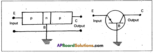
Working of p-n-p transistor : The base part is made of n-type, emitter and collector parts are ‘made of p-type. The circuit symbol of p-n-p transistor is shown in figure.
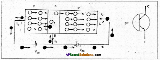
The emitter junction is forward biased by connecting positive terminal off battery to the emitter and negative to the base. The collector junction is reverse biased by connecting negative to fee collector and positive to fee base.
The holes in p-region (emitter) are repelled by the positive terminal and crossing the emitter junction, enter the base region causing emitter current IE. Few holes are combined with electrons in base region, this constitute base current (IB). Majority of holes enters through the collector region. The negative terminal battery rapidly sweeps the holes in the collector region causing collector current (IC).
IE = IB – IC
In p-n-p transistor inside the circuit charge carriers are holes and outside the circuit charge carriers are electrons.
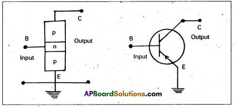
n-p-n transistor: If the base part is made of p-type, emitter and collector parts are made of n-type, we get n-p-n transistor. The circuit symbol of n-p-n transistor is shown in figure.
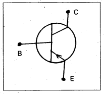
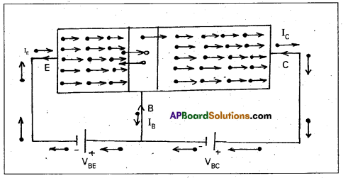
The emitter junction is forward biased with negative end of a battery connected to emitter and positive to the base. The collector junction is reverse biased with collector positive end of a battery and negative to the base.
The electrons in the emitter (n-region) are repelled by the negative terminal of a battery and cross the base region constituting the emitter current IE. A small number of electrons may recombine with holes in base region constituting base current IB.
Majority charge carriers (electrons) enters into the collector region. The positive terminal of battery rapidly sweeps the electrons in collector, constituting collector current IC.
IE = IB + IC
In n-p-n transistor charge carriers inside and outside the circuit are electrons.
![]()
Question 5.
What is amplification ? Explain the working of a common emitter amplifier with necessary diagram.
Answer:
Amplification : The process of raising the strength of a weak signal is called amplification and the device which accomplishes this job is called an amplifier.
Amplifiers are of two types.
- Power amplifier
- Voltage amplifier.
Amplification factor: The ratio between output voltage to the input voltage is called amplification factor.
A = \(\frac{v_0}{v_i}\)
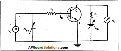
Common emitter transistor amplifier:
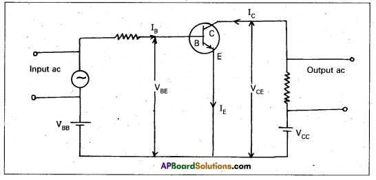
The n-p-n common emitter amplifier circuit is shown in figure. In this circuit the battery VBB provides the biasing voltage VBE for the base emitter junction. The emitter junction is forward biased and the battery VCC provides the biasing voltage VCE for the emitter collector junction. The junction is reverse biased. Most of the electrons from emitter cross the base region and move into the collector.
The input signal to be amplified is connected in series with the biasing battery (VBB). A load resistance RL is connected in the collector circuit and output voltage is taken across RL.
As the base emitter voltage (VBE) changes due to input signal, the base current changes (IB) . This results in large change in collector current (ΔIC). The change in collector emitter voltage (ΔVCE) is taken across RL. Thus amplified output is obtained across RL.
Current gain (β) : The ratio of change in collector current to the change in base current is called current gain (or) current amplification factor.
β = \(\frac{\Delta \mathrm{I}_{\mathrm{C}}}{\Delta \mathrm{I}_{\mathrm{B}}}\)
Voltage gain (AV) : It is the ratio of change in output voltage (ΔVCE) to the change in input voltage (ΔVBE).
Power gain : It is defined as the product of current gain and voltage gain.
Power gain (Ap) = Current gain × Voltage gain.
Question 6.
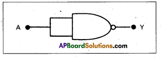
Draw an OR gate using two diodes and explain its operation. Write the truth table and logic symbol of OR gate.
Answer:
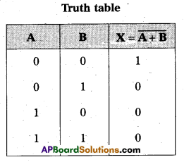
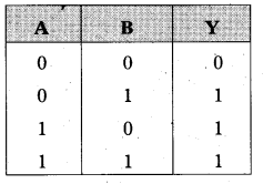
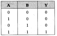
OR Gate : It has two input terminals and one output terminal. If both inputs are low the output is low. If one of the inputs is high, or both the inputs are high then the output of the gate is high. The truth tables of OR gate.
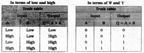
In truth table logic function is written as A or B ‘OR’ logic function is represented by the symbol ‘plus’
Q = A + B
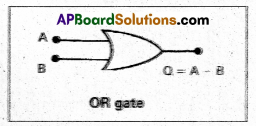
Logic gate ‘OR’ is shown given below.
Implementation of OR gate using diodes:
Let D1 and D2 be two diodes.
A potential of 5V represents the logical value 1
A potential of 0V represents the logical value 0
When A = 0, B = 0 both the diodes are reverse, biased and there no current through the resistance. So, the potential at Q is zero. i.e. Q = 0. When A = 0 or B = O and the other equal to a potential of 5V i.e., Q = 1. When both A and B which is 5V i.e., Q = 1. The output is same as that of the OR gate.
Question 7.
Sketch a basic AND circuit with two diodes and explain its operation. Explain how doping increases the conductivity in semiconductors?
Answer:
AND gate : It has two input terminals and one out terminal
- If both the inputs are low (or) one of the inputs is low.
⇒ The out is low in an AND gate. - If both the inputs are high ⇒ The output of the gate is high
Note: If A and B are the inputs of the gate and the output is ‘Q’ then ‘Q‘ is a logical function of A and B.
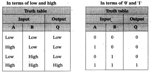
AND gate Truth Tables
The logical function AND is represented by the symbol dot so that the output, Q = A.B and the circuit symbol used for the logic gate AND is shown in Fig.
The logical function AND is similar to the multiplication.
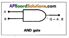
Implementation of AND gate using diodes: Let D1 and D2 represents two diodes. A potential of 5 V represents the Logical value 1 and a potential of 0 V represents the logical value zero (O). When A = 0, B = 0 both the diodes D1 and D2 are forward-biased and they behave like closed switches. Hence, the output Q is same as that A or B(equal to zero.) When A = 0 or B = 0, D1 or D2 is forward – biased and Q is zero. When A = 1 and B = 1 both the diodes are reverse – biased and they behave like open switches. There is no current through the resistance R making the potential at Q equal to 5V i.e., Q = 1. The output is same as that of an AND gate.
Doping increases the conductivity in Semiconductors : If a pentavalent impurity (Arsenic) is added to a pure tetravalent semiconductor it is called n-type semiconductor. Arsenic has 5 valence electrons, but only 4 electrons are needed to form covalent bonds with the adjacent Germanium atoms. The fifth electron is very loosely bound and become a free electron. Therefore excess electrons are available for conduction and conductivity of semiconductor increases.
Similarly when a trivalent impurity Indium is added to pure Germanium it is called p-type semiconductor. In this excess holes in addition to those formed due to thermal energy are available for conduction in the valence bând and the conductivity of semiconductor increases.
Problems
Question 1.
In a half wave rectifier, a p-n junction diode with internal resistance 20 ohm is used. If the load resistance of 2 ohm is used in the circuit, then find the efficiency of this half wave rectifier.
Solution:
Internal resistance (rf) = 20Ω
RL = 2kΩ = 2000 Ω
η = \(\frac{0.406 R_L}{r_f+R_L}\) = \(\frac{0.406 \times 2000}{20+2000}\) × 100 = \(\frac{812 \times 100}{2020}\)
η = 40.2%
![]()
Question 2.
A full wave p-n junction diode rectifier uses a load resistance of 1300 ohm. The internal resistance of each diode is 9 ohm. Find the efficiency of this full wave rectifier.
Solution:
Given that RL = 1300 Ω
rf = 9Ω
η = \(\frac{0.812 \mathrm{R}_{\mathrm{L}}}{\mathrm{r}_{\mathrm{f}}+\mathrm{R}_{\mathrm{L}}}\) = \(\frac{0.812 \times 1300}{9+1300}\) × 100
η = \(\frac{8120 \times 13}{1309}\)
η = 80.64%
Question 3.
Calculate the current amplification factor β(beta) when change in collector current is 1mA and change in base current is 20μA.
Solution:
Change in collector current (ΔIC) = 1mA = 10-3 A
Change in base current (ΔIB) = 20μA = 20 × 10-6 A
β = \(\frac{\Delta \mathrm{I}_{\mathrm{C}}}{\Delta \mathrm{I}_{\mathrm{B}}}\) = \(\frac{10^{-3}}{20 \times 10^{-6}}\)
β = \(\frac{1000}{20}\)
β = 50
Question 4.
For a transistor amplifier, the collector load resistance RL = 2k ohm and the input resistance Ri = 1 k ohm. If the current gain is 50, calculate voltage gain of the amplifier.
Solution:
RL = 2kΩ = 2 × 10³ Ω
Ri = 1kΩ = 1 × 10³ Ω
β = 50.
Voltage gain (AV) = β × \(\frac{\mathrm{R}_{\mathrm{L}}}{\mathrm{R}_{\mathrm{i}}}\) = \(\frac{50 \times 2 \times 10^3}{1 \times 10^3}\)
AV = 100.
Textual Exercises
Question 1.
In an n-type silicon, which of the following statement is true :
(a) Electrons are majority carriers and trivalent atoms are the dopants.
(b) Electrons are minority carriers and pentavalent atoms are the dopants.
(c) Holes are minority carriers and pentavalent atoms are the dopants.
(d) Holes are majority carriers and trivalent atoms are the dopants.
Answer:
(c). In an n-type semiconductor, it is obtained by doping the Ge or Si with pentavalent atoms. In n-type semiconductors, electrons are majority carriers and holes are minority carriers.
Question 2.
Which of the statements given in Exercise 1 is true for p-type semiconductors ?
Answer:
(b) & (d). p-type semiconductor is obtained by doping Ge or Si with trivalent atoms. In p-type semiconductor holes are majority carriers and electrons are minority carriers.
Question 3.
Carbon, silicon and germanium have four valence electrons each. These are characterised by valence and conduction bands separated by energy band gap respectively equal to (Eg)c, (Eg)Si and (g)Ge. Which of the following statements is true ?
(a) (Eg)Si < (Eg)Ge < (Eg)C
(b) (Eg)C < (Eg)Ge > (Eg)Si
(c) (Eg)C > (Eg)Si > (Eg)Ge
(d) (Eg)C = (Eg)Si = (Eg)Ge
Answer:
(c). The energy band – gap is largest for carbon, less for sillicon and least for Germanium.
![]()
Question 4.
In an unbiased p-n junction, holes diffuse from the p-region to n-region because
(a) free electrons in the n-region attract them.
(b) they move across the junction by the potential difference.
(c) hole concentration in p-region is more as compared to n-region.
(d) All the above.
Answer:
(c). In an unbiased p-n junction, the diffusion of charge carriers across the junction takes place from higher concentration to lower concentration. Therefore, hole concentration in p-region is more as compared to n-region.
Question 5.
When a forward bias is applied to a p-n junction, it
(a) raises the potential barrier.
(b) reduces the majority carrier current to zero.
(c) lowers the potential barrier.
(d) None of the above.
Answer:
(c). When a forward bias is applied across the p-n junction, the applied voltage opposes the barrier voltage. Due to this, the potential barrier across the junction is lowered.
Question 6.
For transistor action, which of the following statements are correct:
(a) Base, emitter and collector regions should have similar size and doping concentrations.
(b) The base region must be very thin and lightly doped.
(c) The emitter junction is forward biased and collector junction is reverse biased.
(d) Both the emitter junction as well as the collector junction are forward biased.
Answer:
(b) and (c). For a transistor β = \(\frac{\mathrm{I}_{\mathrm{C}}}{\mathrm{I}_{\mathrm{B}}}\)
IB = \(\frac{I_C}{\beta}\) (Or) Rinput = \(\frac{V_{\text {input }}}{V_B}\) = \(\frac{V_{\text {input }}}{I_C}\) . β. i.e., Rinput ∝ \(\frac{1}{\mathrm{I}_{\mathrm{C}}}\)
Therefore Rinput is inversly proportional to the collector current. For high collector current, the Rinput should be small for which the base region must be very thin and lightly doped for a transistor action, the emitter junction is forward biased and collector junction is reverse biased.
Question 7.
For a transistor amplifier, the voltage gain
(a) remains constant for all frequencies.
(b) is high at high and low frequencies and constant in the middle frequency range.
(c) is low at high and low frequencies and Constant at mid frequencies.
(d) None of the above.
Answer:
(c). The voltage gain is low at high and low frequencies and constant at mid-frequency.
Question 8.
In half-wave rectification, what is the output frequency, if the input frequency is 50 Hz. What is the output frequency of a full-wave rectifier for the same input frequency ?
Answer:
A half wave rectifier rectifies only the half of ac input i.e., it conducts once during an ac input cycle while a full wave rectifier rectifies both the half cycles of the ac input i.e., it conducts twice during a cycle.
The output frequency for half-wave is 50Hz.
The output frequency of a full-wave rectifier is 2 × 50 = 100Hz.
Question 9.
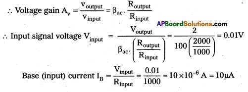
For a CE-transistor amplifier, the audio signal voltage across the collected resistance of 2 kΩ is 2 V. Suppose the current amplification factor of the transistor is 100, find the input signal voltage and base current, if the base resistance is 1 kΩ.
Solution:
Given, collector resistance Routput = 2KΩ = 2000Ω.
Current amplification factor of the transistor βAC = 100.
Audio signal voltage Voutput = 2V
Input (base) resistance Rinput = 1KΩ = 1000Ω
Question 10.
Two amplifiers are connected one after the other in series (cascaded). The first amplifier has a voltage gain of 10 and the second has a voltage gain of 26. If the input signal is 0.01 volt, calculate the output ac signal.
Solution:
Given, voltage gain of first Amplifier, \(\mathrm{A}_{\mathrm{V}_1}\) = 10
Voltage gain of second Amplifier, \(\mathrm{A}_{\mathrm{V}_2}\) = 20
Input voltage V1 = 0.01V
Total voltage gain Av = \(\frac{v_0}{v_i}\) = \(\mathrm{A}_{\mathrm{V}_1}\) × \(\mathrm{A}_{\mathrm{V}_2}\)
\(\frac{v_0}{0.01}\) = 10 × 20; V0 = 2V
Question 11.
A p-n photodiode is fabricated from a semiconductor with band gap of 2.8 eV. Can it detect a wavelength of 6000 nm ?
Solution:
Energy(E) = \(\frac{h c}{\lambda}\) = \(\frac{6.6 \times 10^{-34} \times 3 \times 10^8}{6000 \times 10^{-9} \times 1.6 \times 10^{-19}}\) eV = 2.06 eV.
The band – gap is 2.8 eV and energy E is less than band gap (E < Eg). So p-n junction cannot detect, file radiation of given wavelength 6000 nm.
Additional Exercises
Question 1.
The number of silicon atoms per m3 is 5 × 1028. This is doped simultaneously with 5 × 10²² atoms per m3 of Arsenic and 5 × 1028 per m3 atoms of Indium. Calculate the number of electrons and boles. Gives that n,sub>i = 1.5 × 10¹⁶ m-3. Is the material n-type or p-type ?
Solution:
We know that for each atom doped of arsenic one free electron is received. Similarly, for each- atom doped of Indium a, vacancy is crested So, the number of free electrons introduced by pentavalent impurity added.
ne = NAs = 5 × 10²²m3 —- (i)
The number of holes introduced by trivalent impurity added.
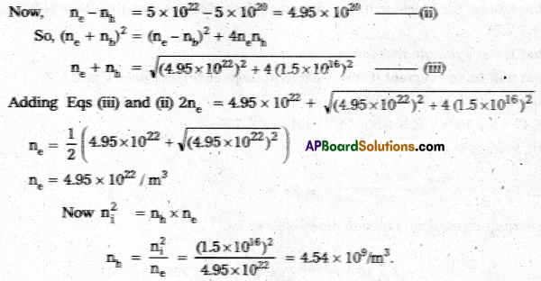
As number of electrons ne (= 4.95 × 10²²) is greater than number of holes nh (= 45 × 109). So, the material is n-type semiconductor.
Question 2.
In an intrinsic semiconductor the energy gap Eg is 1.2 eV. Its hole mobility is much smaller than electron mobility and independent of temperature. What is the ratio between conductivity at 600K and that at 300 K ? Assume that the temperature dependence of intrinsic carrier concentration ni is given by ni = n0 exp \(\left(-\frac{\mathbf{E}_{\mathbf{g}}}{2 \mathbf{K}_{\mathbf{B}} \mathbf{T}}\right)\) where n0 is a constant.
Solution:
Given, intrinsic carrier concentration ni = \(n_0 e^{-E g / 2 k_B T}\) and Energy gap Eg = 1.2 eV
KB = 8.62 × 10⁻⁵ eV/K
For T = 600k
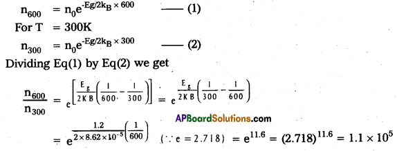
Let the conductivities are σ600 and σ300 (∵ σ = e n µe)
\(\frac{\sigma_{600}}{\sigma_{300}}\) = \(\frac{n_{600}}{n_{300}}\) = 1.1 × 10⁵.
![]()
Question 3.
In a p-n junction diode, the current I can be expressed as I = I0 exp \(\left(\frac{e V}{2 K_B T}-1\right)\) where I0 is called the reverse saturation current, V is the voltage across the diode and is positive for forward bias and negative for reverse bias, and I is the current through the diode, kB is the Boltzmann constant (8.6 × 10⁻⁵ eV/K) and T is the absolute temperature. If for a given diode I0 = 5 × 10-12 A and T = 300 K, then
(a) What will be the forward current at a forward voltage of 0.6 V ?
(b) What will be the increase in the current if the voltage across the diode is increased to 0.7 V?
(c) What is the dynamic resistance ?
(d) What will be the current if reverse bias voltage changes from IV to 2 V ?
Solution:
Given I0 = 5 × 10-12 A, T = 300K
KB = 8.6 × 10⁻⁵eV/K = 8.6 × 10-5 × 1.6 × 10-19 J/K
a) Given, voltage V = 0.6V
\(\frac{\mathrm{eV}}{\mathrm{K}_{\mathrm{B}} \mathrm{T}}\) = \(\frac{1.6 \times 10^{-19} \times 0.6}{8.6 \times 10^{-5} \times 1.6 \times 10^{-19} \times 300}\) = 23.26
The current I through a junction diode is given by
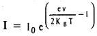
= 5 × 10-12(e23.26 – 1) = 5 × 10-12 (1.259 × 10¹⁰ – 1)
= 5 × 10-12 × 1.259 × 1010 = 0.063 A
Change in current ΔI = 3.035 – 0.063 = 2.9A
b) Given voltage V = 0.7 V
\(\frac{\mathrm{eV}}{\mathrm{K}_B T}\) = \(\frac{1.6 \times 10^{-19} \times 0.7}{8.6 \times 10^{-5} \times 1.6 \times 10^{-19} \times 300}\) = 27.14
Now, I = \(I_0 e^{\frac{e V}{K_B T}}-1\) = 5 × 10-12(e27.14 – 1)
= 5 × 10-12(6.07 × 10¹¹ – 1)
= 5 × 10-12 × 5.07 × 1011 = 0.035 A
Change in current ΔI = 3.035 – 0.693 = 2.9 A
c) ΔI = 2.9A, voltage ΔV = 0.7 – 0.6 = 0.1 V
Dynamic retistance Rd = \(\frac{\Delta \mathrm{V}}{\Delta \mathrm{I}}\) = \(\frac{0.1}{2.9}\) = 0.0336Ω
d) As the voltage changes from IV to 2V, the current I will be almost equal to
I0 = 5 × 10-12A.
It is due to that the diode possesses practically infinite resistance in the reverse bias.
Question 4.
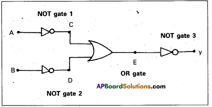
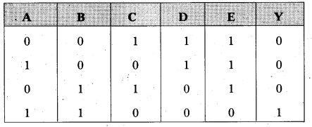
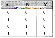
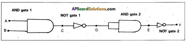
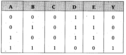
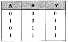
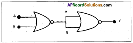
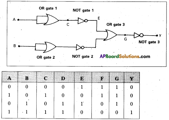
You are given the two circuits as shown in Fig.Show that circuit (a) acts as OR gate while the circuit (b) acts as AND gate.
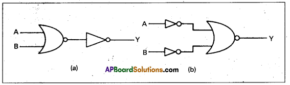
Solution:
a) Split the gate, OR gate
The truth table :
Here, for given A and B as inputs, C is the output of OR gate and input of NOT gate 1, D is the output of NOT gate 1 and input of NOT gate 2, then Y is finally output.
This is same as OR gate. So, this circuit acts as OR gate.
b) Split the gate:
The truth table:
Here, for given A and B as inputs, C is the output of A and D is the output of B, E is the output of OR gate and input of NOT gate 3, then Y is finally output. .
This is same as AND gate, So the given circuit acts as AND gate
Question 5.
Write the truth table for a NAND gate connected as given in fig.
Hence identify the exact logic operation carried out by the circuit.
Solution:
Split the gate:
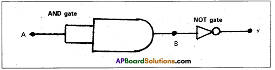
Truth table:
B is the output of AND gate and input of NOT gate.
So, for input A and output Y, the table is
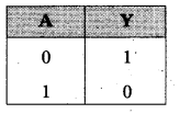
Here, it is same as NOT gate, so the logic operation is carried by this circuit as NOT gate
Question 6.
You are given two circuits as shown in fig. which consist of NAND gates. Identify the logic operation carried out by the two circuits.
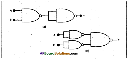
Solution:
a) Split the gate:
C is the output of AND gate 1 and input of NOT gate 1, D is the output of NOT gate 1 and input of AND gate 2, E is the õut put of AND gate 2 and input of NOT gate 2, Y is finally output
Truth table:
So, this logic operation is AND gate.
b)
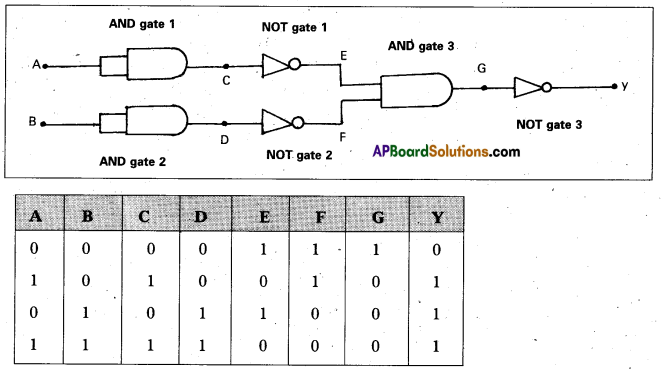
C is the out put of AND gate 1
D is the out put of AND gate 2
E is the out put of NOT gate 1
F is the out put of NOT gate 2
G is the out put of AND gate 3 and input of NOT gate 3
Here, it is same as OR gate. A and B are inputs and Y is output.
So, this logic operation resembles to OR gate.
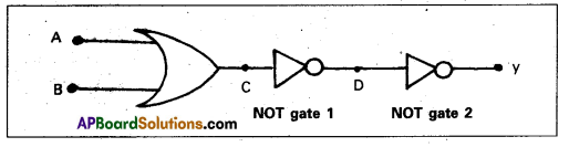
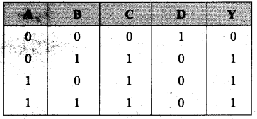
Question 7.
Write the truth table for circuit given in fig. below consisting of NOR gates and identify the logic operation (OR, AND, NOT) which this circuit is performing.
Hint: A = 0, B = 1 then A and B inputs of second NOR gate will be 0 and hence Y = 1. Similarly work out the values of Y for other combinations of A and B. Compare with the truth table of OR, AND, NOT gates and find the correct one.)
Solution:
Split the gate:
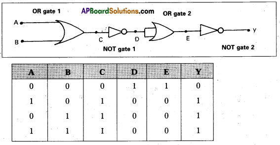
C is the output of OR gate 1.
D is the output of NOT gate 1 and input of NOT gate 2. E is the output of OR gate 2 and input of the NOT gate 2. Here, it is same as OR gate. A and B are inputs and Y is output.
So, this logic operation resembles to OR gate.
![]()
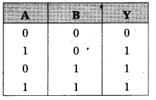
Question 8.
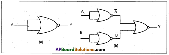
Write the truth table for the circuits given in fig. consisting of NOR.gates ònly. Identify the logic operations (OR, AND, NOT) performed by the two circuits.
Solution:
a) Split the gate
B is the output of OR gate and input of NOT gate. So, the gate resembles to NOT gate as A is input and Y is output.
b) a) Split the gate:
C is the output of OR gate 1 and input of NOT gate 1, D is the output of OR gate 2 and input of NOT gate 2, E is the output of NOT gate 1, F is the output of NOT gate 2.
G is the output of OR gate 3 and input of NOT gate 3. The truth table resembles to AND gate as A and B inputs and Y is output.
This operation is AND gate.